Thin Wafer Market Snapshot

Key Players

  • LG Siltron (South Korea)
  • Shin-Etsu Chemical (Japan)
  • GlobalWafers (Taiwan)
  • SUMCO Corporation (Japan)
  • Siltronic (Germany)
  • S.O.I.TEC Silicon On Insulator Technologies (France)
  • EV Group (Austria)
  • Applied Materials (United States)
  • Disco Corporation (Japan)
  • 3M (United States)

Market Size

Base Year 2024
$11.98 Bn
CAGR
7.52%
Forecast 2034
$24.74 Bn

Market Segments

By Material Type
  • Silicon
  • Gallium Arsenide
  • Silicon Carbide
By Thickness
  • Less than 100 Micrometers
  • 100 to 300 Micrometers
  • Above 300 Micrometers
By Application
  • Semiconductor Devices
  • Optoelectronics
  • MEMS
  • Others

Market Dynamics

Drivers
  • Increasing demand in electronics
  • Technological advancements in wafer production
Restraints
  • High production costs
  • Limited technology advancements
Opportunities
  • Rapid technological advancements
  • Increasing demand for miniaturized devices

Market Size

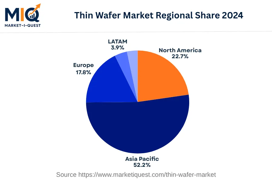
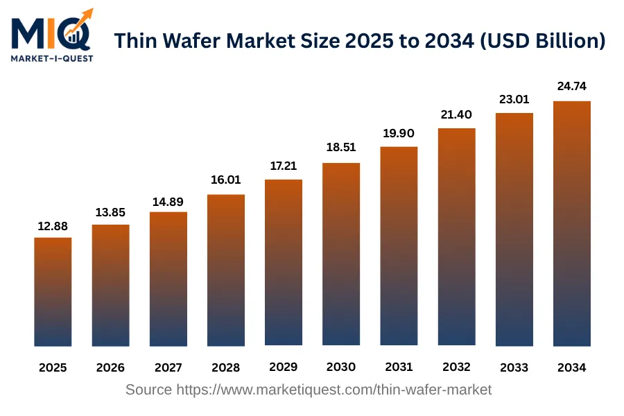
The Thin Wafer market is expected to grow in size from USD 12.88 billion in 2025 to USD 24.74 billion by 2034. This growth corresponds to a CAGR of 7.52%. This market's expansion trajectory is characterized by a steady growth trajectory from USD 11.98 billion in 2024 to nearly doubled value by the end of 2034. Market growth during this period is driven by the progression of the year 2025 as a starting point, setting a foundation for growth that gradually increases over the subsequent decade. On the regional distribution front, in the year 2024, the market share is predominantly influenced by the Asia Pacific's contribution of 52.2%. North America and Europe followed with respective shares of 22.7% and 17.8%. The remainder of the market in this timeframe is divided among Latin America and the Middle East & Africa, contributing 3.9% and 3.4% respectively. Herein, the proportions present an overview of the Thin Wafer market's geographical distribution as it prepares for nearly a decade of anticipated growth.

Key Takeaways

  • By Material Type - Silicon led the domain holding the majority share in 2024.
  • By Thickness - 100 to 300 Micrometers held the most significant share in 2024.
  • By Applications - Semiconductor Devices emerged at the forefront making up the largest share in 2024.
thin-wafer-market market size

Key Driving Factors

Shift Towards Compact Electronic Devices

In recent years, major electronics manufacturers are focusing on designing compact and lightweight devices. This trend towards miniaturization stresses on the need for smaller but efficient components. By virtue of their thin structure, wafers perfectly fit into this requisite, prompting an increase in their market demand. The thin wafer market is being driven substantially by this shift in device manufacturing. Thin wafer technology enables manufacturers to produce smaller chips, without compromising on their performance, ultimately making the end-product sleek and desirable by consumers. This trend is prevalent across industries like mobile devices, consumer electronics, automotive, and medical, among others.

Increasing Use in Renewable Energy Sector

The rapid adoption of renewable energy technologies, particularly solar energy, presents another driving factor. High-performance thin wafers are critical to the efficiency of solar cells. With governments worldwide encouraging renewable energy implementation to achieve sustainability targets, the demand for thin wafers in the manufacture of photovoltaic cells has seen an upsurge. Solar energy companies are investing heavily in thin wafer technologies that can enhance sunlight absorption and improve energy conversion rates without adding significant cost. As countries continue to expand their renewable energy grid, the thin wafer market is expected to benefit in parallel.

Market Evolution by Timeline

2019-2023
Throughout 2019–2023, main buyers of thin wafers were largely concentrated within the high-end consumer electronics and automotive industries, particularly in regions of East Asia and North America. Companies' push towards compact technology and improved performance pushed usage rates. Availability and integration were facilitated with the maturity of thin film deposition techniques. Constraints were typically seen in fragile handling methods and extreme thinness of the wafer. Regulatory factors, like environmental standards, obliged players to adopt low-waste, efficient manufacturing processes, heralded by programs like the EU Ecodesign. Commercially, most deals involved bulk supply contracts, and partnerships were common among material suppliers and technology companies. The uncertainty of silicon price variation prompted risks, with companies responding by investing in silicon alternatives such as gallium nitride.
2024
In 2024, demand evident, especially in North America, for thin wafers in renewable energy applications, photovoltaic cells being a major use case. Technology developed around stack designs, with manufacturing capacity constraints surfacing from advanced etching techniques. The California Solar Mandate, which requires solar panels on new homes, played a critical role in expanded product application. More companies switched to leasing models, offering customers cost-effective options. However, supply chain interruptions due to the COVID-19 pandemic were a significant risk factor, leading to a reevaluation of long-term contracts and a push for industrial self-reliance.
2025-2029
From 2025 to 2029, demand patterns showed a rise in the demand for thin wafers in Internet of Things (IoT) applications and AI-based solutions within wider sectors, such as healthcare and energy management in Europe and Asia Pacific. Improved etching and automation techniques facilitated greater production volumes, but access to rare earth elements showed signs of constraints. Meanwhile, programs like the EU's Horizon 2020 promoted advanced materials development. Transactional contracts became more common as price competition increased. Increased trade tensions emerged as a potential risk, prompting companies to seek diversified supply sources and regional partnerships.
2030-2034
In the period 2030–2034, demand for thin wafers continued to rise in cloud computing and telecommunication sectors. Mature supply chains with innovations in manufacturing, such as atomic layer etching, were realized, although ensuring consistent quality at scale remained a challenge. New standards such as the ISO 45001 material handling standard emerged that had a significant impact on wafer handling techniques. Flat-rate, long-term contracts became a prevalent commercial model, providing stability for manufacturers. Polarization of supply chains became a concern due to geopolitical factors, leading to the need for companies to reassess risk management strategies.

Future Market Outlook

Future Opportunities

The robust demand for thin wafers has created multiple opportunities across various industries as of 2023. The automotive sector is increasingly leaning on thin wafer technology, particularly for electric vehicles, where companies like Tesla explore lightweight materials to enhance performance. Concurrently, the aerospace sector is witnessing advancements in thin wafers aimed at reducing the weight of components while maintaining high durability standards set by bodies like the FAA. The ongoing trend toward renewable energy technologies, including solar panels, has led firms like First Solar to investigate thin film technologies, promising efficiency improvements. Moreover, the Consumer Technology Association predicts that enhancements in smart devices will necessitate thinner architectures, driving demand for advanced wafers. Countries like Japan and South Korea are actively investing in research initiatives to bolster their semiconductor industries, presenting opportunities for collaboration and knowledge sharing. In academic circles, partnerships such as that between MIT and various semiconductor companies aim to refine thin substrate applications, which could yield significant breakthroughs in form-factor designs. As regulations around electronic waste become increasingly stringent globally, the focus on sustainable production methods will heighten interest in thin wafers for their recyclable properties, paving the way for expanded market applications. These factors suggest a fertile landscape for innovation and expansion in the thin wafer sector, spurred by technological evolution and a concerted push for sustainability.

Segmentation Analysis

By Material Type

The market is divided into subsegments including Silicon, Gallium Arsenide, and Silicon Carbide. Silicon accounted for the largest revenue share while Gallium Arsenide is expected to grow at the fastest CAGR during the forecast period.

Largest Revenue Share

Silicon

Market Share Leader

The silicon subsegment remained dominant in revenue terms primarily due to its wide-ranging applications and inherent properties. Silicon semiconductors are ubiquitous and find extensive application in almost all electronic devices because of their superior electrical properties and optimal cost. The subsegment benefits from entrenched market structures and high switching costs as silicon has been an industry standard for decades. Geographically, the demand is driven by regions with strong technology industries, like the United States and Asia-Pacific. The regulatory environment also plays a role, with developed markets having more stringent standards for electronic components, encouraging the use of high-quality, silicon-based components. The silicon market also enjoys strong supply regulatory protection driving its growth.

Fastest CAGR

Gallium Arsenide

Forecast Period Growth Leader

Gallium Arsenide, despite its smaller current market share, shows the most promising growth trajectory. The high growth is due to increasing application in specific high-growth areas like high-frequency 5G infrastructure, where the high electron mobility of Gallium Arsenide is valued. High-speed data communication applications value the superior speed and frequency characteristics of Gallium Arsenide over alternatives. As the technology matures and economies of scale set in, the adoption barriers are expected to lower significantly. However, higher acquisition costs and complex manufacturing processes are near-term risks that could impact the expected growth trajectory. Given the rise of the 5G infrastructure and the era of superfast communication, Gallium Arsenide can potentially disrupt silicon's longstanding dominance if it overcomes these formidable initial barriers.

By Thickness

The market is divided into subsegments including less than 100 micrometers, 100 to 300 micrometers, and above 300 micrometers, with the 100 to 300 micrometers segment accounting for the largest revenue share, while the less than 100 micrometers segment is expected to grow at the fastest CAGR during the forecast period.

Largest Revenue Share

100 to 300 Micrometers

Market Share Leader

The 100 to 300 micrometers segment dominates the market in revenue terms, primarily driven by its versatility across a wide array of applications. Its thickness provides an optimal balance between efficiency and functionality, making it highly sought-after in industries such as electronics, packaging, or medical devices. Furthermore, this segment has benefited from regulatory standards in several jurisdictions, which often stipulate minimum thickness levels for safety or performance reasons. Demand within the segment is further underpinned by geographical factors, notably the fast-growing demand in developing markets, where regulation is becoming more stringent. Its cost-effectiveness and widespread availability have also contributed to its leading position. Channels of distribution are well established in this segment, minimizing any potential switching costs, while further innovations in production technology promise to keep driving demand and revenue growth.

Fastest CAGR

Less than 100 Micrometers

Forecast Period Growth Leader

The fastest-growing subsegment is less than 100 micrometers. It's seeing increasing adoption due to new technological advancements enhancing the desirability of thinner materials. These advancements have helped overcome traditional barriers to adoption such as fragility, leading to an exponential growth in potential use cases. This trend is further catalyzed by increasingly stringent environmental regulations, prompting companies to reduce material consumption wherever possible. Furthermore, significant capital expenditure by major industry players, alongside key partnerships aimed at driving scale and reducing costs, are set to fuel growth. However, the subsegment faces near-term risks, including the challenge of maintaining product integrity at such low thickness levels and the potential for disruptive innovation in alternate materials or technologies.

By Application

The market is divided into subsegments including Semiconductor Devices, Optoelectronics, MEMS, and Others. In the base year of 2024, Semiconductor Devices accounted for the largest revenue share while Optoelectronics is expected to grow at the fastest CAGR.

Largest Revenue Share

Semiconductor Devices

Market Share Leader

Semiconductor Devices led the revenue of the market segment in 2024. The rationale behind this dominance lies in the extensive and ever-growing use of semiconductor devices in various industries such as automotive, electronics, healthcare, and more. With a continuous push towards digitization, the need for semiconductor devices has significantly grown. Additionally, their role in enabling technology-driven solutions, from embedding intelligence in consumer electronics and industrial equipment to data processing in the cloud, further bolsters their demand. The increasing investments and advancements in semiconductor technology and the global push towards energy-efficient solutions are some factors boosting their market growth. Geographically, markets like Asia Pacific, the hub of electronics production, contribute majorly to the revenue of semiconductor devices. External factors, like favorable government policies and regulations promoting semiconductor manufacturing, are also influencing revenue shares.

Fastest CAGR

Optoelectronics

Forecast Period Growth Leader

On the other hand, Optoelectronics is projected to witness the fastest growth during the forecast period. This rapid growth can be attributed to its widespread adoption in various applications such as LED lighting, solar cells, and photodiodes, which are increasingly employed in consumer electronics, telecommunications, and automotive industries. Key drivers for this expected growth are technological innovations, capex in R&D, and partnerships among major companies. Barriers to adoption could include the technology's high cost and the need for specialized skills for its integration. Nonetheless, policy incentives like tax benefits for renewable energy technologies (such as solar photovoltaic) and growing environmental awareness may serve as a catalyst to overcome these barriers. While the high initial investment and geopolitical uncertainties could pose near-term risks, the long-term outlook remains favorable with increasing adoption in emerging applications like Li-Fi and electric vehicles.

Competitive Analysis

Key Market Players

Manufacturers / OEMs

Shin-Etsu Chemical Co., Ltd.
Japan
Sumco Corporation
Japan
Siltronic AG
Germany

Key Suppliers & Raw Materials

GCL Group
China
LKAB Minerals
Sweden
Ferroglobe
UK

Distributors, Integrators & Channel Partners

Arrow Electronics, Inc.
US
Avnet, Inc.
US
WPG Holdings
Taiwan

Porter’s Five Forces Analysis

This analysis offers a comprehensive view of the competitive dynamics within the Thin Wafer market.

Supplier Bargaining Power

High

Limited suppliers and specialized equipment maintain high supplier power in the market.

Buyer Bargaining Power

Medium

High product differentiation reduces buyers' bargaining power, but large buyers can leverage volume.

Threat of Substitutes

Low

The unique characteristics of thin wafers make substitutes less viable.

Threat of New Entrants

High

Low regulatory barriers, but significant CapEx and expertise needed, enable high threat of new entrants.

Competitive Rivalry

High

Intense competition among major players and continuous technological advancement fuel high competitive rivalry.

Regional Analysis

Geographic market dynamics and growth opportunities across key regions

Global Market Outlook

thin-wafer-market market regional share

North America

In 2024, the North American thin wafer market stood as a dynamic segment with significant contribution to the semiconductor industry. Technological adoption contributed expansively, with key players heavily investing in research and development for more efficient wafer designs. Regulations in the U.S., Canada, and Mexico also catalyzed market growth, facilitating ease of operations for wafer manufacturers. Prices remained competitive, providing a robust supply-demand equilibrium, benefiting buyers, and incentivizing producers. Trends included a shift in enterprise buyer behavior towards thin wafers of smaller sizes to optimize device performance and portability. There was a noticeable emphasis on partnerships and mergers to maximise resources, particularly in the U.S., where technology giants strengthened their market footholds. The industry also witnessed significant product shifts with the wider integration of solar wafers used in utilities and manufacturing sectors.

In the healthcare sector, the demand for thin wafers for revolutionary medical micro-devices and MEMS increased. As a result, manufacturers tailored their supply to cater specifically to this surge. Retail consumers showed preference towards devices that featured thin wafer technology, notable in products launched in 2024 by market-leading tech firms. The underlying push in the North American thin wafer market in 2024 revolved around harnessing technology for improved performance, cost-efficiency, and innovative applications across varied sectors.

Asia Pacific

The Thin Wafer market in Asia Pacific exhibited significant growth in 2024, influenced by industry-specific drivers and multiple market trends. Key drivers behind this growth were the rising demand for low-power, high-performance electronic devices, along with a surge in investment in semiconductor technologies from leading economies such as China, India, and Japan. The market was also propelled by supply dynamics that saw smaller ASEAN markets ramping up production capacities to meet increasing demand, and broader regional adoption of advanced manufacturing techniques in producing thin wafers.

Market trends witnessed were largely influenced by shifts in buyer behavior, with an increasing preference for compact and lightweight electronic devices, fostering greater demand for thin wafers. Significant product innovation in semiconductor technology also contributed to this trend. Channel dynamics also underwent notable change, with partnerships and M&A activities increasing among key players to enhance market reach and strengthen product portfolios. Regulatory bodies across the region enforced stricter standards to ensure product quality and sustainability, playing a substantial role in shaping market trends. These developments particularly impacted sectors that relied heavily on advanced electronics, including enterprise, healthcare, utilities, retail, manufacturing, and government sector. For instance, manufacturing sector embraced smart automation, leading to higher demand for thin wafers, whilst healthcare sector’s increasing reliance on medical electronic appliances provided a stimulating effect on market dynamics in 2024.

Europe

In the 2024 base year, Thin Wafer Market in Europe showed considerable dynamism primarily driven by expanding semiconductor and microelectronic sectors. Miniaturization trend in electronics technology led to high demand for ultra-thin wafers in Germany and the UK, spurred by large electronics manufacturing sectors. Regulatory stimulus in the form of the EU's Green Deal pushed companies towards adopting more energy-efficient wafer technologies. In Italy and Spain, investment in solar power capability led to increased utilization of thin silicon wafers. Consumer trends leaned towards smart and connected devices, leading to growth in thin wafer utilization across the Nordics. The Benelux region saw a surge in strategic alliances and M&A activities, boosting sector growth. A shift towards smarter manufacturing technologies in Central & Eastern Europe increased base demand. The need for high-performance chips in healthcare, telecommunications, and automotive sectors escalated consumption in France and Italy.

In retail, the growing demand for smart POS systems invigorated the thin wafer supply chain. Reliable utility providers in Germany invested heavily in infrastructure, using thin wafers to develop utility metering solutions. Concerning enterprise, data center expansion across Europe required advanced microprocessors and SSDs, thus influencing the market. Finally, digital government initiatives across various EU nations ignited further demand, securing the thin wafer market firmly within Europe's technological advancement trajectory.

Latin America

In 2024, the Thin Wafer Market in Latin America exhibited considerable dynamism, strongly instigated by technological advancements and varied end-use applications. Increased adoption of thin wafer technology in sectors such as healthcare, enterprise, and manufacturing in countries like Brazil, Mexico, and Argentina was instrumental to market growth. Regulatory measures promoting the use of thin wafers for enhancing product efficiency and reducing silicon waste further drove demand. Additionally, significant investments in thin wafer production equipment and advanced packaging tools, especially by Colombia and Chile, underpinned overall market progression. However, supply dynamics were partially dampened due to fluctuations in raw material pricing that affected production costs.

Changing buyer behavior reflected a preference for energy-efficient and miniaturized electronic devices, steering innovations and shifts in the product landscape. Brazil led this charge, witnessing substantial uptake of Internet of Things applications and devices utilizing thin wafers. There was also recognition of the need for strategic alliances and M&As in the region to achieve operational efficiencies. Examples include partnerships for producing extremely thin and less power-consuming circuits in Peru. Compliance with international standards also emerged as a key trend, with countries like Argentina enforcing policies for the use of the latest thin wafer production technology. Consequently, the thin wafer market reported a significant competitive edge in LATAM's electronics industry for 2024.

Middle East & Africa

The Thin Wafer Market in the Middle East and Africa in 2024 was predominantly driven by advancing semiconductor technology, increased electronics production, and government initiatives in countries such as Saudi Arabia, UAE, Qatar, Egypt, and South Africa. Significant investments in technology sectors and the push for digitization created a surge in demand for thin wafers. Furthermore, strong regulations in environmental management, particularly in Israel, affected the increase in the use of thin wafers, preferred due to their less energy consumption and lower waste generation.

Global technology shifts significantly impacted the market in 2024, with a notable increase in demand for thin wafer products in telecom, utilities, and manufacturing sectors. The wide-scale adoption of 5G infrastructure, particularly in UAE, underscored this growth. There was a visible trend of strategic partnerships between local firms and global wafer manufactures for better market penetration. For instance, Saudi Arabia's oil and gas giant Aramco entered into partnership deals with international wafer manufacturers for its digital transformation. Lastly, the stringent enforcement of Saudi Arabia's Vision 2030 policy led to rapid technological modernization, fueling the demand for thin wafer technology in the country's financial services and retail sectors.

Recent Industry Developments

Latest market innovations, product launches, and strategic initiatives

May 2026

Gaoce Co., Ltd. announced it has the capability to deliver small batches of 60-80 μm silicon wafers and has taken the lead in launching 50 μm ultra-thin silicon wafers, which have begun sample delivery and testing.

April 2025

Black Semiconductor acquired Applied Nanolayers to boost energy-efficient chip technology, leveraging ANL's graphene expertise.

Frequently Asked Questions